

Support our independent tech coverage. Chrome Unboxed is written by real people, for real people—not search algorithms. Join Chrome Unboxed Plus for just $2 a month to get an ad-free experience, access to our private Discord, and more. Learn more about membership here.
START FREE TRIAL (MONTHLY)START FREE TRIAL (ANNUAL)
If you’ve been keeping an eye on the upcoming Googlebook laptops from Google, you likely know about the handful of device manufacturers and chip makers that are on board for actual device launches this fall. Acer, ASUS, HP, Dell, and Lenovo will be working in tandem with MediaTek, Qualcomm and Intel to deliver the first wave of Googlebooks in just a few months. But there are already more devices in development and on the way.
One specific processor codename that has me pretty excited for the second wave of Googlebook devices is one we’ve talked a little bit about around here: ‘Calypso’ (alongside its reference baseboard, ‘Mensa’).
I spent some time last week digging into the exact engineering commits surrounding this chip as I try to make sense of what this SoC will be. While we know it is Qualcomm in origin, I couldn’t find anything I could decipher when it comes to understanding which Snapdragon brand we’re looking at here.
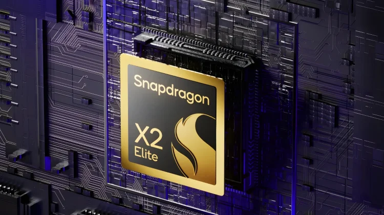
So I called in Gemini. I asked Google’s AI to look through everything I could find with ‘Calypso’ and while I can’t conclusively nail down the retail branding just yet, Gemini makes a solid case that points to one definitive conclusion: ‘Calypso’ isn’t a budget mobile chip. It points instead to Qualcomm’s next-generation flagship laptop silicon: the Snapdragon X2 Plus or X2 Elite.
Splitting the “CPUCP” binaries
In Qualcomm’s silicon architecture, CPUCP stands for CPU Control Processor. This is not a standard software feature; it is a dedicated, hardware-isolated microcontroller embedded directly inside Qualcomm’s highest-end compute platforms. Its sole job is to manage core clustering, heavy-duty power scaling, and intense thermal throttling independently of the main operating system.
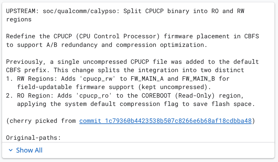
The fact that Calypso explicitly utilizes and partitions a CPUCP binary tells us it is running Qualcomm’s custom, heavy-compute Oryon CPU architecture. You simply don’t find a dedicated CPU control processor on lightweight mobile chips or low-end budget silicon.
Expanding the “ROMSTAGE” memory limits
Another massive technical breadcrumb Gemini found is an increase in the romstage region size. In coreboot development, the romstage is the critical early phase of the boot process responsible for initializing system memory (RAM). When developers are forced to physically increase the size of this region, it is because the initialization code and pre-loaded firmware binaries have grown too large for standard limits.
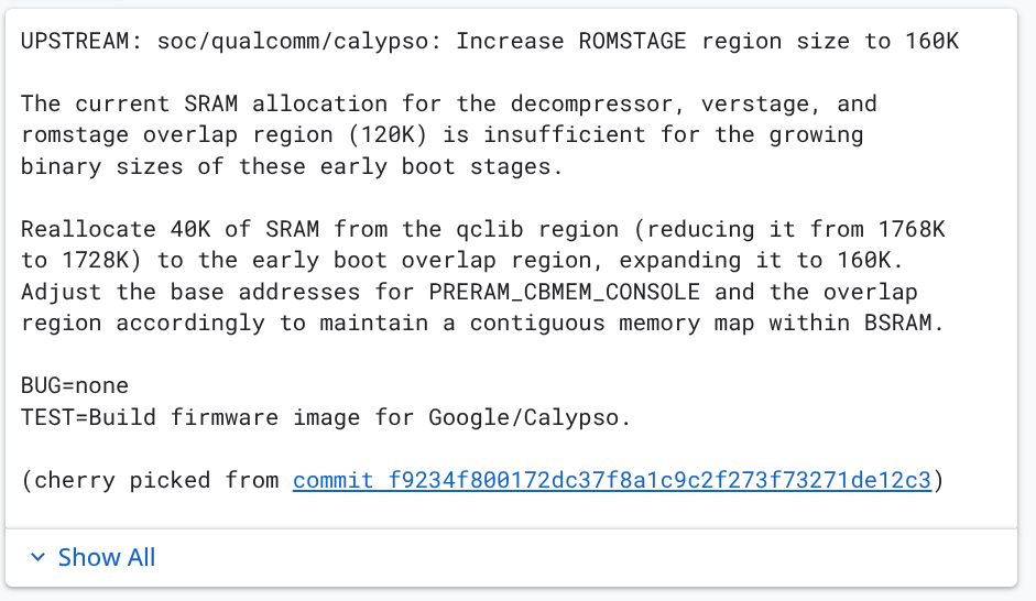
A low-end chip designed for a cheap, basic laptop wouldn’t carry an early firmware footprint dense enough to start running out of room in the bootblock. This kind of code expansion happens when a chip has a massive amount of high-performance memory channels, deep hardware caches, and complex silicon blocks that need to be woken up the absolute second the computer turns on.
Activating “Delta DCB” support
DCB stands for Device Configuration Block. In display engineering, DCB structures are the precise firmware instructions used to initialize and map out incredibly complex video pipelines. Specifically, “delta DCB” allows the system to dynamically calculate and route video signals for multi-display setups, high-refresh-rate external monitors, and premium high-bandwidth eDP (embedded DisplayPort) laptop panels.
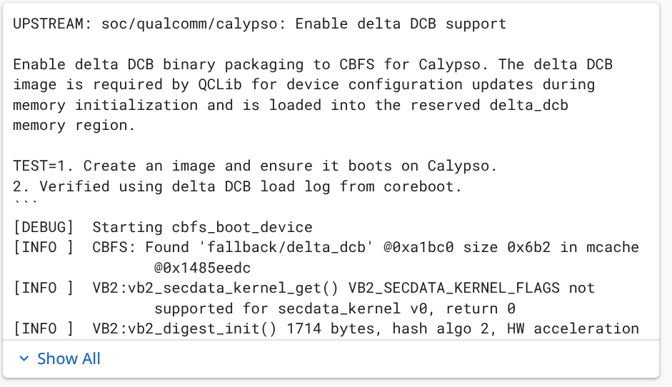
A chip designed for this sort of use case isn’t generally put into low-end laptops that aren’t expected to drive higher-end displays and more than one external at a time. While this clue isn’t a standalone proof that ‘Calypso’ is a high-end SoC, it is a helpful hint for sure.
Switching to “Non-Secure Blobs” for testing
When chipmakers are in the early stages of waking up a brand-new processor platform, they utilize specialized, closed-source firmware packages (often referred to as “blobs,” such as Qualcomm’s qclib). Switching to “non-secure” variations of these blobs allows engineers to bypass rigid security lockdowns during development so they can test raw hardware communication.
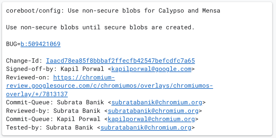
Qualcomm only deploys this specific, multi-layered initialization blob architecture for its premium, PC-class Compute platforms. It requires an extensive firmware footprint just to wake up the deep hardware caches, complex memory controllers, and massive neural processing sub-systems that define high-end laptop silicon. Again, not a 100% correlation, but a solid hint.
Connecting the dots to Snapdragon X2
With all this info on the table, you get an unmistakable picture. ‘Calypso’ is initializing PCIe lanes, expanding its early boot memory to accommodate heavy firmware, loading desktop-class display routing, and utilizing hardware-isolated CPU controllers.
If the current “Bluey” chips we’ve tracked in the repository (that are coming this fall) represent the first-generation Snapdragon X Plus tier, everything about ‘Calypso’ we know thus far tracks as its direct architectural successor.
Given that Qualcomm has already officially confirmed it is partnering with Google to power premium, AI-forward devices arriving this fall, Calypso is almost certainly the engineering code name for the Snapdragon X2 Plus or a custom implementation of the Snapdragon X2 Elite. Google isn’t just building a casual web browser companion for its next major software chapter; they are working hand-in-hand with Qualcomm to ensure their new desktop environment is anchored by an absolute powerhouse of a flagship processor.
SUBSCRIBE TO UPSTREAM
Get Chrome Unboxed delivered straight to your inbox
Upstream is our flagship, curated newsletter with the top stories, most click-worthy deals, giveaways, and trending articles from Chrome Unboxed sent directly to your inbox a few times a week. Join 31,000+ subscribers.